Design and Production of PCBs
The production of PCBs is specialized in complex multi-layer (up to 18 layers) PCBs by small lots (mainly, of about 500 sq dm) and double-sided PCBs of 3-5 Accuracy Classes as per the GOST R 53429 as well as Class E as per the SN (above Class 5).
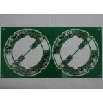
| SSB |
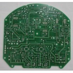
DSB |
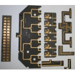
PCBs for SHF |
MLB |
 |
 |
 |
 |
- - Critical parameters
- - PCB thickness: 0.2-3.0 mm;
- - max. dimensions of PCB: 400 580 mm (of workpiece – 420,600 mm);
- - through-hole plating;
- - direct plating;
- - identification making by using screen-printed technique, accuracy ± 0.15 mm;
- - laser photo-plotter mask-making (raster unit – 12.7 m; max. film size – 648,530 mm);
- - scribing.
- - Basic materials
- - foreign dielectric, thickness 0.1-3.0 mm with foil thickness 5; 9; 18; 35 m
|
- - Critical parameters
- - PCB thickness: 0.2-3.0 mm;
- - max. dimensions of PCB: 400 580 mm (of workpiece – 420,600 mm);
- - through-hole plating;
- - direct plating;
- - identification making by using screen-printed technique, accuracy ± 0.15 mm;
- - laser photo-plotter mask-making (raster unit – 12.7 m; max. film size – 648,530 mm);
- - scribing.
- - Basic materials
- - TLY –type materials
|
- - Critical parameters
- - up to 26 layers;
- - PCB thickness: 0.4-3.0 mm;
- - max. dimensions of PCB: 400,520 mm (of workpiece – 420,600 mm);
- - MPCB with inner and external heat sinks;
- - through-hole plating;
- - direct plating;
- - identification making by using screen-printed technique, accuracy ± 0.15 mm;
- - laser photo-plotter mask-making (raster unit – 12.7 m; max. film size – 648,530 mm);
- - scribing.
- - Basic materials
- - foreign fiberglass of 48; 63; 100; 180 m thickness;
- - Russian-made and foreign copper foil of 18 m thickness, in rolls;
- - Russian-made copper foil of up to 180 m thickness for inner heat sinks.
|
Basic Parameters of PCBs
- - Compliance with Standards
- - 4-5 Accuracy Classes as per the GOST R 53429:
- - minimum diametre of plated holes – 0.1 mm;
- - minimum guarantee belt – 0.025 mm;
- - minimum size of conductor/clearance – 0.1/0.1 mm;
- - rate of hole diameter/ board thickness– 1::10.
- - Group of Rigidity 4 as per the GOST 23752 for climatic factors:
- - ambient temperature
-60 … +120°С
- - temperature difference
-60 … +120°С
- - relative air humidity
95-98% at temperature of (40±2)°С
- - Coating Finishing
- - galvanic and chemigold plating, HAL (POS-63);
- - galvanic nickel-plating;
- - local electroplating of pattern;
- - protection solder mask – ELPEMER GL2467 liquid double-component composition by PETERS Company.
- - Quality Control
- - computer-aided optical check;
- - electrical check;
- - check of impedance.
Technology
- - computer-aided design;
- - computer-aided production-engineering;
- - computer-aided production-control;
- - environmental safety;
- - advanced method for control of manufacturing operations and complete products;
The production technology ensures the production of up to 800,000 sq m of PCBs a year, at that the product range is up to 900 types.
Order Terms and Cost
The prices of the manufacture of PCBs can vary depending on the complexity of works, the technological features of PCBs as well as the order amount. If the order amount is more than 4,000 sq dm for one position, the price is negotiated. At that, the production engineering and electrical check are free of charge.
Terms of order fulfillment:
- - for double-sided PCBs – 1-3 weeks;
- - for multi-layer PCBs – 2-4 weeks..
There is a system of rush orders performed according specially negotiated terms.
Contacts:
Chief of Research-and-Production Complex – Oleg E. Stepanov:
phone: +7 (8422) 262 254 fax: +7 (8422) 262 961
Chief of Laboratory for PCBs and Coating – Oleg S. Karpusenko:
phone: +7 (8422) 262 369
|
Additional Materials:
Order Form
Order Letter
|
")
")